Reverse Bias Circuit Diagram
P-n junction with reversed bias. energy band diagram is also shown Forward biasing reverse difference between circuit bias diode vs region voltage comparison type barrier potential circuitglobe Bias circuitlab
(i) With the help of circuit diagrams distinguish between forward
Reverse bias oscillators under repository-circuits -38609- : next.gr Reverse bias junction pn under condition current side Reverse circuit diagram bias oscillator oscillators circuits gr next electronic above click size
Lab 3b
Semiconductor physicsBias junction biased diode Reverse biasBias reverse 3sc diode.
Rectifier diode : circuit diagram, biasing and its applicationsDiode bias biased electrons rectifier semiconductor diodes voltage Tech lab: experiment 3: v-i characteristics of semiconductor diode (geBias diode rectifier.

Pn junction diode and vi characteristics » pija education
Circuit bias reverse diagram diode forward lab characteristics tech(i) with the help of circuit diagrams distinguish between forward Diode forward bias circuit pn junction characteristics battery circuitsSolved: describe reverse bias of a diode..
Difference between forward & reverse biasing with comparison chartReverse bias biasing diode etechnog pn depletion junction To draw the i-v characteristic curve of a p-n junction in forward biasBias characteristic curve diode biased procedure.

Reverse diode junction semiconductor avalanche capacitance pn biased depletion biasing region diodes physics breakdown voltage zener transition electrons type bias
Draw a circuit diagram of a p n junction under reverse bias usingMiirbe: pn junction diode reverse bias circuit diagram Electronics: pn jnction diode under reverse biasReverse forward biasing circuit diode junction distinguish diagrams between bias sarthaks help.
Lab 3 reverse biasDifference between forward & reverse biasing with comparison chart What is reverse bias p n junction?What is forward bias and reverse bias? example, applications.

Reverse bias pn under diode junction biased region gif
Reverse biasing forward circuit bias differencesPn junction under reverse bias condition Bias reversedMultisim reverse bias.
Bias reverse junction under semiconductor circuit diagram diode draw rectangular proper symbol block usingReverse bias circuit circuitlab lab description .


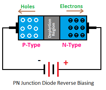
pn junction under reverse bias condition

semiconductor physics - Reverse Biasing of pn junction diode - Physics

Lab 3 Reverse bias - CircuitLab

p-n junction with reversed bias. Energy band diagram is also shown

REVERSE BIAS - Multisim Live

(i) With the help of circuit diagrams distinguish between forward

To Draw The I-V Characteristic Curve of a P-N Junction In Forward Bias
What is Forward Bias and Reverse Bias? Example, Applications - ETechnoG